Despite continuous improvements and incremental upgrades taking place with each new generation, processors haven't had any industry shifting advancements for a long time. The switch from vacuum tubes to transistors was huge. The switch from individual components to integrated circuits was huge. After that though, there haven't been other similar paradigm shifts on that scale.
Yes, transistors have gotten smaller, chips have gotten faster, and performance has increased hundredfold, but we're starting to see diminishing returns...
This is the fourth and last installment in our CPU design series, giving you an overview on computer processor design and manufacturing. Starting from the top down, we looked at how computer code is compiled into assembly language and how that is converted into binary instructions that the CPU can interpret. We looked at how processors are architected and process instructions. Then we looked at the various structures that make up a CPU.
Going a bit deeper, we saw how those structures are built and how the billions of transistors work together inside a processor. We looked at how processors are physically made from raw silicon. We learned the basics of semiconductors and what the inside of a chip really looks like. If you missed any of this, here's an index of the series:
(instruction set architectures, caching, pipelines, hyperthreading)
Part 2: CPU Design Process
(schematics, transistors, logic gates, clocking)
Part 3: Laying Out and Physically Building the Chip
(VLSI and silicon fabrication)
Part 4: Current Trends and Future Hot Topics in Computer Architecture
(Sea of Accelerators, 3D integration, FPGAs, Near Memory Computing)
Moving on to part four. Since companies don't share their research or details of their current technology, it is hard to get a sense of exactly what is in the CPU in your computer. What we can do however, is look at current research and where the industry is headed.
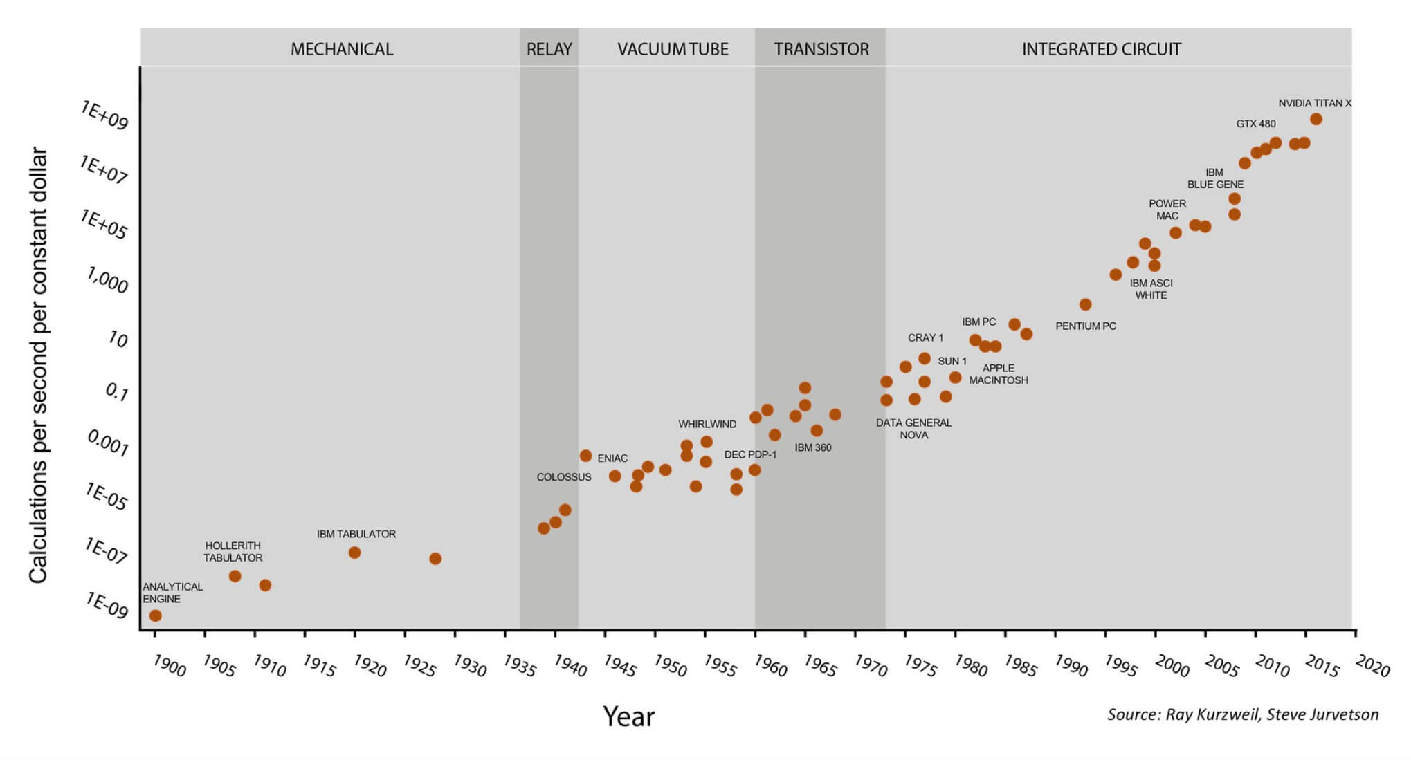
One famous representation of the processor industry is Moore's Law. This describes how the number of transistors in a chip doubles roughly every 18 months. This was true for a very long time, but is starting to slow down. Transistors are getting so small that we are nearing the limit of what physics will allow. Without a groundbreaking new technology, we'll need to explore different avenues to achieve future performance boosts.
Moore's Law over 120 Years
One direct result of this breakdown is that companies have started to increase core count rather than frequency to improve performance. This is the reason we are seeing octa-core processors becoming mainstream rather than 10GHz dual core chips. There simply isn't a whole lot of room left for growth beyond just adding more cores.
On a completely different note, Quantum Computing is an area that does promise lots of room for growth in the future. I'm no expert on this and since the technology is still being created, there aren't many real "experts" anyway. To dispel any myths, quantum computing isn't something that will provide you with 1,000fps in a real-life like render or anything like that. For now, the main advantage to quantum computers is that it allows for more advanced algorithms that were previously not feasible.
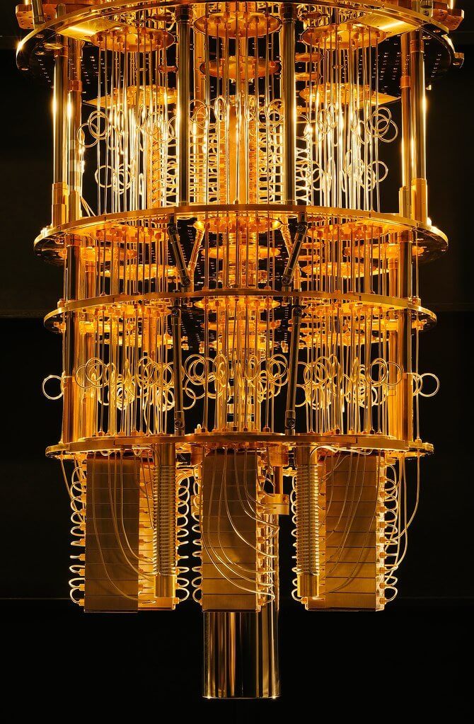
One of IBM's Quantum Computer prototypes
In a traditional computer, a transistor is either on or off which represents a 0 or a 1. In a quantum computer, superposition is possible which means the bit can be both 0 and 1 at the same time. With this new capability, computer scientists can develop new methods of computation and will be able to solve problems we don't currently have the compute capabilities for. It's not so much that quantum computers are faster, it's that they are a new model of computation that will let us solve different types of problems.
The technology for this is still a decade or two away from the mainstream, so what are some trends we are starting to see in real processors right now? There are dozens of active research areas but I'll touch on a few that are the most impactful in my opinion.
A growing trend that we've been impacted by is heterogeneous computing. This is the method of including multiple different computing elements in a single system. Most of us benefit from this in the form of a dedicated GPU in our systems. A CPU is very customizable and can perform a wide variety of computations at a reasonable speed. A GPU, on the other hand, is designed specifically to perform graphics calculations like matrix multiplication. It is really good at that and is orders of magnitude faster than a CPU at those types of instructions. By offloading certain graphics calculations from the CPU to the GPU, we can accelerate the workload. It's easy for any programmer to optimize software by tweaking an algorithm, but optimizing hardware is much more difficult.
But GPUs aren't the only area where accelerators are becoming common. Most smartphones have dozens of hardware accelerators designed to speed up very specific tasks. This computing style is known as a Sea of Accelerators and examples include cryptography processors, image processors, machine learning accelerators, video encoders/decoders, biometric processors, and more.
As workloads get more and more specialized, hardware designers are including more and more accelerators into their chips. Cloud providers like AWS have started providing FPGA cards for developers to accelerate their workloads in the cloud. While traditional computing elements like CPUs and GPUs have a fixed internal architecture, an FPGA is flexible. It's almost like programmable hardware that can be configured to whatever your computing needs are.
If you want to do image recognition, you can implement those algorithms in hardware. If you want to simulate how a new hardware design will perform, you can test it on the FPGA before actually building it. An FPGA offers more performance and power efficiency than GPUs, but still less than an ASIC (application specific integrated circuit). Other companies like Google and Nvidia are developing dedicated machine learning ASICs to speed up image recognition and analysis.
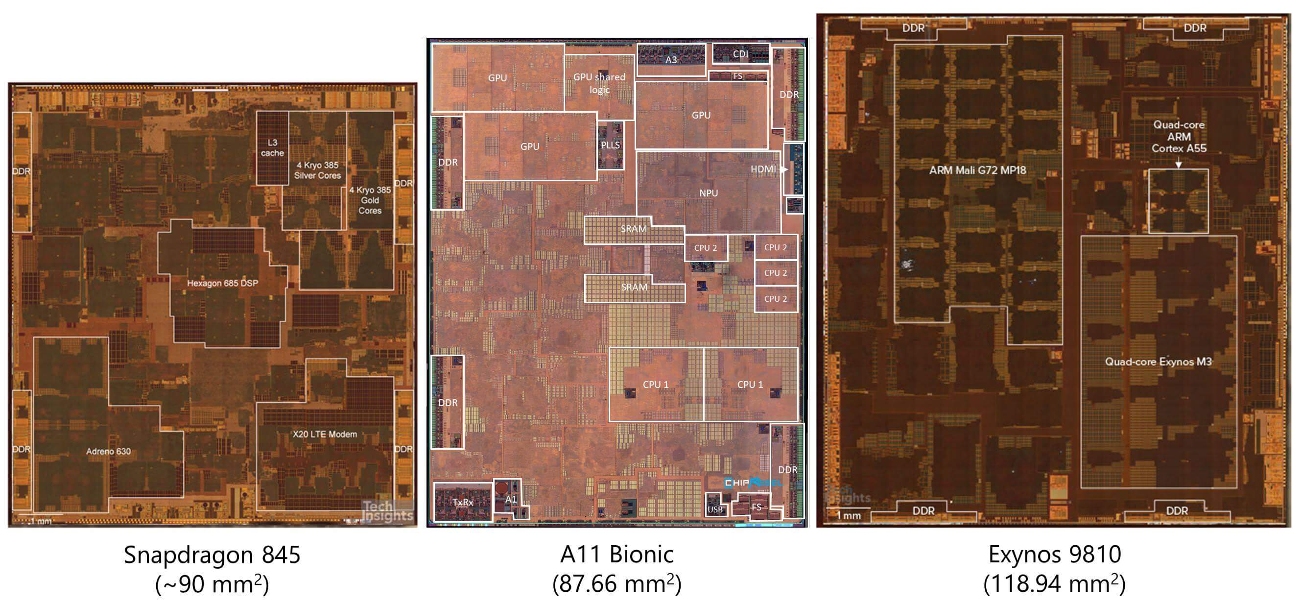
Die shots showing the makeup of several common mobile processors
Looking at the die shots of some fairly recent processors, we can see that most of the area of the CPU is not actually the core itself. A growing amount is being taken up by accelerators of all different types. This has helped speeding up very specialized workloads in addition to the benefit of huge power savings.
Historically, if you wanted to add video processing to a system, you'd just add a chip to do it. That is hugely inefficient though. Every time a signal has to go out of a chip on a physical wire to another chip, there is a large amount of energy required per bit. On its own, a tiny fraction of a Joule may not seem like a lot, but it can be 3-4 orders of magnitude more efficient to communicate within the same chip versus going off chip. We have seen the growth of ultra low power chips thanks to the integration of these accelerators into the CPUs themselves.
Accelerators aren't perfect though. As we add more of them to our designs, chips become less flexible and start to sacrifice overall performance for peak performance in certain workloads. At some point, the whole chip just becomes a collection of accelerators and then it isn't a useful CPU anymore. The tradeoff between specialized performance and general performance is always being fine tuned. This disconnect between generalized hardware and specific workloads is known as the specialization gap.
While some think we may be at the peak of a GPU / Machine Learning bubble, we can likely expect more of our computations to be offloaded to specialized accelerators. As the cloud and AI continue to grow, GPUs appear to be our best solution so far to achieve the massive amounts of compute needed.
Another area where designers are looking for more performance is memory. Traditionally, reading and writing values has been one of the biggest bottlenecks for processors. While fast, large caches can help, reading from RAM or your SSD can take tens of thousands of clock cycles. Because of this, engineers often view memory access as more expensive than the actual computation itself. If your processor wants to add two numbers, it first needs to calculate the memory addresses where the numbers are stored, find out what level of the memory hierarchy has the data, read the data into registers, perform the computation, calculate the address of the destination, and write back the value to wherever it is needed. For simple instructions that may only take a cycle or two to complete, this is extremely inefficient.
A novel idea that has seen a lot of research is a technique called Near Memory Computing. Rather than fetching small bits of data from memory to bring to the fast processor for compute, researchers are flipping this idea around. They are experimenting with building small processors directly into the memory controllers on your RAM or SSD. By doing the computation closer to the memory, there is the potential for huge energy and time savings since data doesn't need to be transferred around as much. The compute units have direct access to the data they need since they are right there in the memory. This idea is still in its infancy, but the results look promising.
One of the hurdles to overcome with near memory computing is manufacturing process limitations. As covered in Part 3, the silicon fabrication process is very complex with dozens of steps involved. These processes are typically specialized to produce either fast logic elements or dense storage elements. If you tried to create a memory chip using a compute-optimized fabrication process, you would have extremely poor density in the chip. If you tried to build a processor using a storage fabrication process, you would have very poor performance and timing.
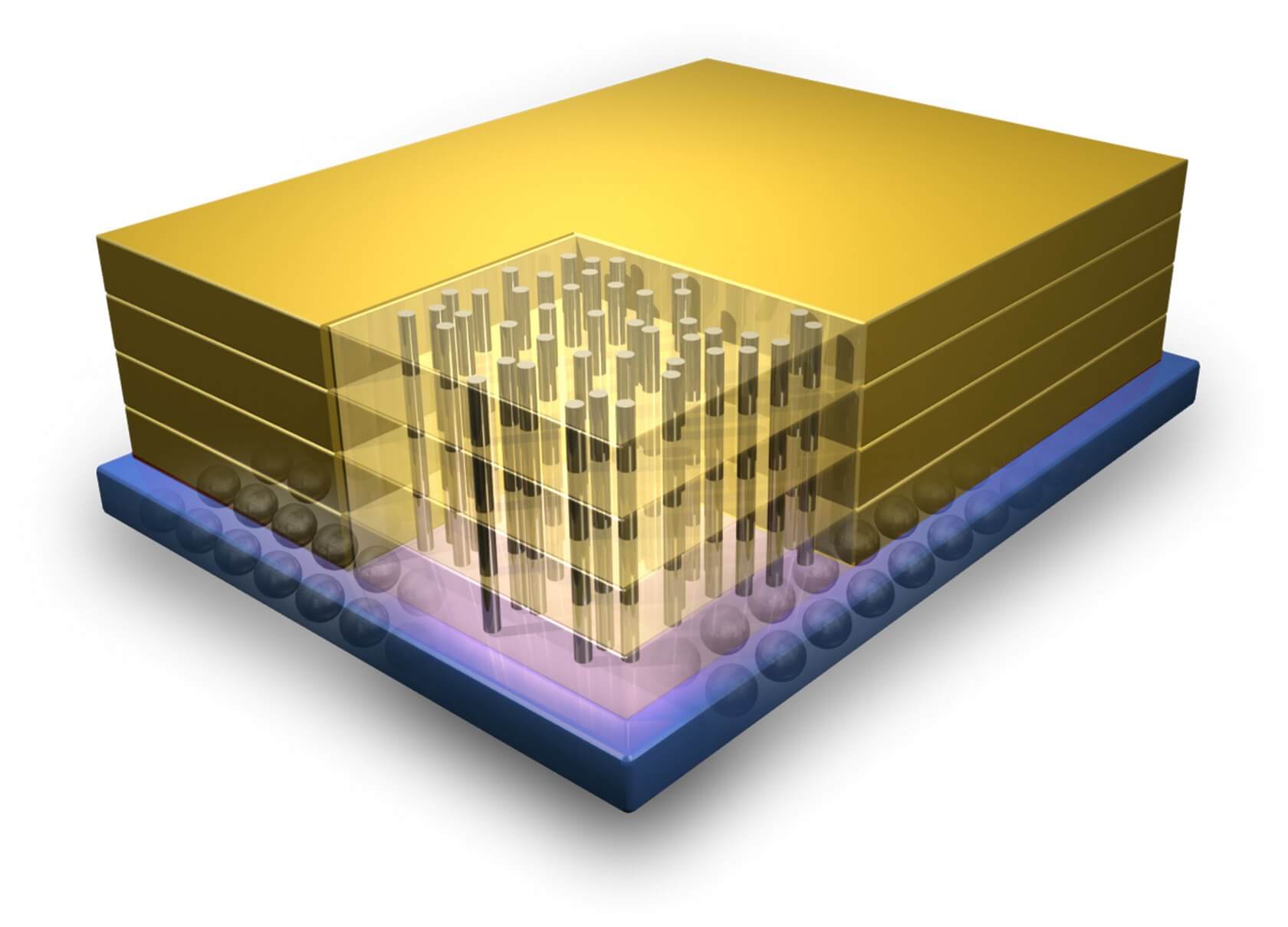
An example of 3D integration showing the vertical connections between transistor layers.
One potential solution to this issue is known as 3D Integration. Traditional processors have one very wide layer of transistors, but this has its limitations. As the name implies, 3D Integration is the process of stacking several layers of transistors on top of each other to improve density and reduce latency. Vertical columns built on different manufacturing processes can then be used to connect between the layers. This idea was proposed a long time ago but the industry lost interest because of major difficulties in its implementation. Recently, we have seen 3D NAND storage technology and a resurgence of this as a field of study.
In addition to physical and architectural changes, one trend that will affect the entire semiconductor industry is a greater focus on security. Until recently, security in our processors was somewhat of an afterthought. This is similar to the how the internet, email, and many other systems we rely on were designed with almost no regard to security. Any security present now was bolted on after the fact to make us feel safer. With processors, this has come back to bite companies, particularly Intel.
The Spectre and Meltdown bugs are perhaps the most famous example of designers adding features that greatly speed up a processor, despite not fully understanding the security risks involved. Current processor design is placing a much greater emphasis on security as a key part of the design. With increased security there often comes a performance hit, but given the harm these major security bugs can have, it's safe to say that we are better off focusing just as much on security as we do on performance.
In previous parts of this series, we touched on techniques such as High Level Synthesis that allow designers to first specify their designs in a high level programming language, and then have advanced algorithms determine the optimal hardware configuration to carry out that function. As design cycles get vastly more expensive each generation, engineers are looking for ways to help speed up their development. Expect this trend of software-aided hardware design to continue to grow in its capabilities down the road.
While it's impossible to predict the future, the innovative ideas and research fields we have talked about here should serve as a roadmap for what we can expect in future processor designs. What we can say for sure, is that we are nearing the end of regular manufacturing process improvements. To continue to increase performance each generation, designers will need to come up with even more complex solutions.
We hope this four-part series has piqued your interest in the fields of processor design, manufacturing, verification, and more. There's a never-ending amount of material to cover and each one of these articles could fill an upper level university course if we tried to cover it all. Hopefully you've learned something new and have a better understanding of how complex computers are at every level. If you have suggestions for topics you'd like us to take a deep dive into, we're always open to suggestions.
(instruction set architectures, caching, pipelines, hyperthreading)
Part 2: CPU Design Process
(schematics, transistors, logic gates, clocking)
Part 3: Laying Out and Physically Building the Chip
(VLSI and silicon fabrication)
Part 4: Current Trends and Future Hot Topics in Computer Architecture
(Sea of Accelerators, 3D integration, FPGAs, Near Memory Computing)
Masthead credit: Computer processor with abstract lighting by Dan74
