Now that we know how processors work at a high level, it's time to dig inside to understand how the internal components are designed. This article is the second part in our series on processor design. If you haven't read part one yet, you'll want to go over that first or else some of the concepts in here won't make sense.
(instruction set architectures, caching, pipelines, hyperthreading)
Part 2: CPU Design Process
(schematics, transistors, logic gates, clocking)
Part 3: Laying Out and Physically Building the Chip
(VLSI and silicon fabrication)
Part 4: Current Trends and Future Hot Topics in Computer Architecture
(Sea of Accelerators, 3D integration, FPGAs, Near Memory Computing)
As you probably know, processors and most other digital technology are made of transistors. The simplest way to think of a transistor is of a controllable switch with three pins. When the gate is on, electricity is allowed to flow through the transistor. When the gate is off, current can't flow. Just like the light switch on your wall, but much smaller, much faster, and able to be controlled electrically.
There are two main types of transistors used in modern processors: pMOS and nMOS. An nMOS transistor allows current to flow when the gate is charged or set high, and a pMOS transistor allows current to flow through when the gate is discharged or set low. By combining these types of transistors in a complementary way, we can create CMOS logic gates. We won't get into the nitty gritty details of how transistors physically work in this article, but we'll touch on it in Part 3 of the series.
A logic gate is a simple device that takes inputs, performs some operation, and outputs a result. For example, an AND gate will turn its output on if and only if all the inputs to the gate are on. An inverter or NOT gate will turn its output on if the input is off. We can combine these two to create a NAND or not-and gate which turns its output on if and only if none of the inputs are on. There are other gates with different logic functionality like OR, NOR, XOR, and XNOR.
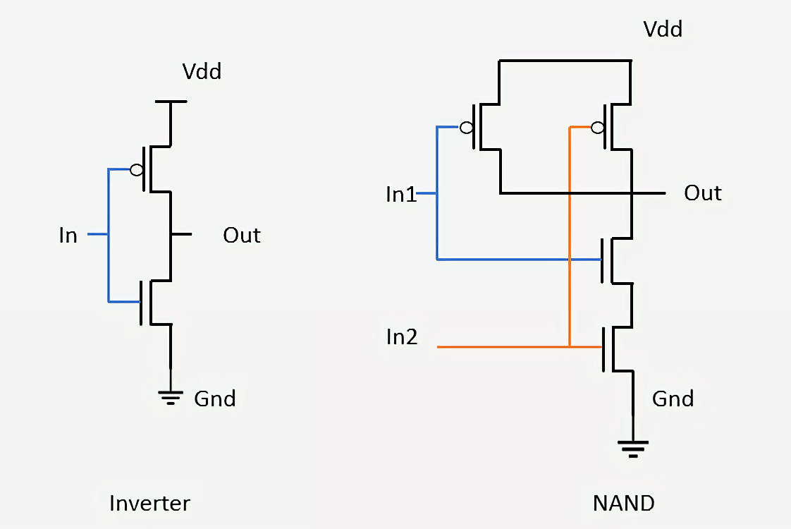
Below we can see how two basic gates are designed from transistors: an inverter and a NAND gate. In the inverter, there is a pMOS transistor on top connected to the power line and an nMOS transistor on the bottom connected to ground. The pMOST transistors are drawn with a small circle connecting to their gate. Since we said that pMOS devices conduct when the input is off and nMOS devices conduct when the input is on, it is easy to see that the signal at Out will always be the opposite of the signal at In. Looking at the NAND gate, we see that it requires four transistors and that the output will be on as long as at least one of the inputs is off. Connecting transistors to form simple networks like this is the same process used to design more advanced logic gates and other circuitry inside processors.
With building blocks as simple as logic gates, it can be difficult to see how they are transformed into a functioning computer. This design process involves combining several gates to create a small device that may perform a simple function. You can then connect many of these devices to form something that performs a slightly more advanced function. The process of combining individual components to create a working design is exactly what is used today to create modern chips. The only difference is that a modern chip has billions of transistors.
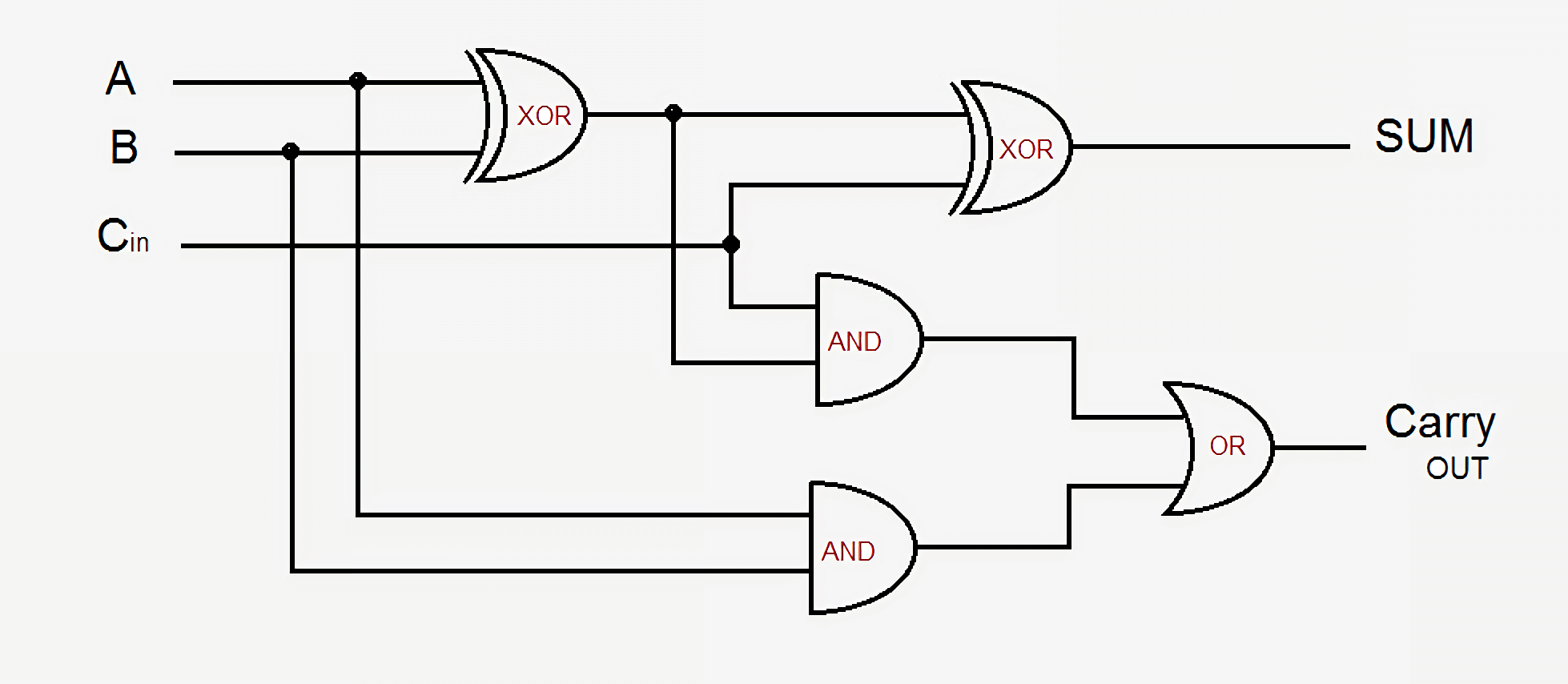
For a quick example, we'll look at a basic adder 1-bit full adder. It takes three inputs - A, B, and Carry-In, and produces two outputs - Sum and Carry-Out. The basic design uses five logic gates and they can be linked together to create any size adder you want. Modern designs improve on this by optimizing some of the logic and carry signals, but the fundamentals are still the same.
The Sum output is on if either A or B is on but not both, or if there is a carry-in signal and either A and B are both on or both off. The carry-out is a bit more complex. It is active when either A and B are both on at the same time, or if there is a carry-in and one of A or B is on. To connect multiple 1-bit adders to form a wider adder, we just need to connect the carry out of the previous bit to the carry in of the current bit. The more complex the circuits get, the messier the logic gets, but this is the simplest way to add two numbers. Modern processors use more complex adders, but those designs are too complicated for an overview like this. In addition to adders, processors also contain units for division, multiplication, and floating-point versions of all of these operations.
Combining a series of gates like this to perform some function on inputs is known as Combinational Logic. This type of logic isn't the only thing found in computers though. It wouldn't be very useful if we couldn't store data or keep track of the state of anything. To do this, we need sequential logic which has the ability to store data.
Sequential logic is built by carefully connecting inverters and other logic gates such that their outputs feed back to the input of the gates. These feedback loops are used to store one bit of data and are known as Static RAM or SRAM. It is called static RAM, as opposed to dynamic in DRAM, because the data being stored is always directly connected to positive voltage or ground.
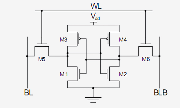
A standard way to implement a single bit of SRAM is with 6 transistors shown below. The top signal, marked WL for Word Line, is the address and when it is enabled, the data stored in this 1-bit cell is sent to the Bit Line, marked BL. The BLB output is known as Bit Line Bar, is just the inverted value of Bit Line. You should be able to recognize the two types of transistors and that M3 and M1 form an inverter along with M4 and M2.
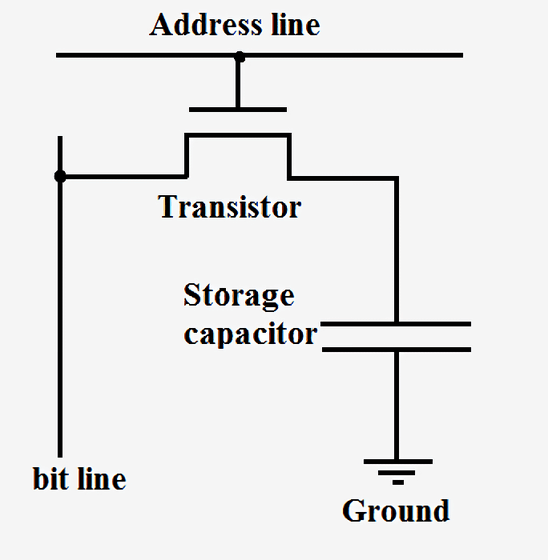
SRAM is what is used to build the super fast caches and registers inside processors. It is very stable, but requires six to eight transistors to store each bit of data. This makes it extremely expensive to produce in terms of cost, complexity, and chip area compared to DRAM. Dynamic RAM, on the other hand, stores data in a tiny capacitor rather than using logic gates. It is called dynamic because the voltage of the capacitor can change dynamically since it is not connected to power or ground. There is just a single transistor that is used to access the data stored in the capacitor.
Because DRAM only requires a single transistor per bit and the design is very scalable, it can be packed densely and cheaply. One drawback to DRAM is that the charge in the capacitor is so small that it needs to be refreshed constantly. This is why when you turn off your computer, the capacitors all drain and the data in your RAM is lost.
Companies like Intel, AMD, and Nvidia certainly don't release schematics for how their processors work, so it's impossible to show full diagrams like this for a modern processor. However, this simple adder should give you a good idea of how even the most complex parts of a processor can be broken down into logic gates, storage elements, and then transistors.
Now that we know how some of the components of a processor are constructed, we need to figure out how to connect everything up and synchronize it. All of the key components in a processor are connected to a clock signal. This alternates between high and low at a predefined interval known as the frequency. The logic inside processor typically switches values and performs calculations when the clock goes from low to high. By synchronizing everything together, we can ensure that data always arrives at the correct time so that there aren't any glitches in the processor.
You may have heard that you can increase the clock to a processor, known as overclocking, to increase its performance. This performance gain comes from switching the transistors and logic inside a processor faster than it was designed for. Since there are more cycles per second, more work can get done and the processor will have a higher performance. This is true up to a certain point though. Modern processors typically run between 3.0GHz and 4.5GHz and that hasn't seemed to change in the past decade. Just like a metal chain is only as strong as the weakest link, a processor can only run as fast as the slowest part. By the end of each clock cycle, every single component in a processor needs to have finished its operation. If any parts aren't done yet, the clock is too fast and the processor won't work. Designers call this slowest part the Critical Path and it is what sets the maximum frequency a processor can run at. Above a certain frequency, the transistors simply cannot switch fast enough and will start glitching or producing incorrect outputs.
By increasing the supply voltage to a processor, we can speed up the switching of the transistors, but that only works up to a certain point as well. If we apply too much voltage, we risk burning up the processor. When we increase the frequency or voltage of a processor, it will always generate more heat and consume more power. This is because processor power is directly proportional to frequency and proportional to the square of voltage. To determine the power consumption of a processor, we usually think of each transistor as a small capacitor that must be charged or discharged whenever it changes value.
Power delivery is such an important part of a processor that in some cases, half of the physical pins on a chip may be just for power or ground. Some chips may pull more than 150 amps at full load and all that current has to be managed extremely carefully. To put this amount of power into perspective, a CPU generates more heat per unit area than a nuclear reactor.
The clock in modern processors accounts for roughly 30-40% of its total power since it is so complex and must drive so many different devices. To conserve energy, most lower-power designs will turn off portions of the chip when they are not in use. This can be done by turning off the clock, known as Clock Gating, or turning off the power, known as Power Gating.
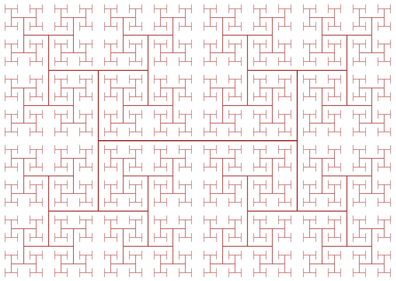
Clocks present another challenge to designing a processor since as their frequencies keep increasing, the laws of physics start getting in the way. Even though the speed of light is extremely fast, it is not fast enough for high-performance processors. If you were to connect the clock to one end of the chip, by the time the signal reached the other end, it would be out of sync by a considerable amount. To keep all portions of the chip in time, the clock is distributed using what is called an H-Tree. This is a structure that ensures all endpoints are the exact same distance from the center.
It may seem extremely tedious and complex to design every single transistor, clock signal, and power connection in a chip, and that would certainly be true. Even though companies like Intel, Qualcomm, and AMD have thousands of engineers, it would not be possible for them to manually design every aspect of a chip. To put together chips on such a scale, they use a variety of advanced tools to generate the designs and schematics for them. These tools will typically take a high level description of what the component should do, and determine an optimal hardware configuration to meet those requirements. There has been a recent trend towards a technique called High Level Synthesis which allows developers to specify the functionality they want in code, and then have computers figure out how to optimally achieve it in hardware.
Just like you can define computer programs through code, designers can also define hardware through code. Languages such as Verilog and VHDL allow hardware designers to express the functionality of whatever circuit they are making. Simulation and verification is done on these designs and if everything passes, they can be synthesized down into the specific transistors that will make up the circuit. While verification may not seem as flashy as designing a new cache or core, it is considerably more important. For every design engineer that a company employs, there may be five or more verification engineers.
Verification of a new design often takes much more time and money than building the actual chip itself. Companies spend so much time and money on verification because once a chip goes into production, there's no way to fix it. With software you can just issue a patch, but hardware doesn't work that way. For example, Intel had a bug in the floating point division unit of some Pentium chips and it ended up costing them the equivalent of $2 billion today.
It can be difficult to wrap your mind around how one chip can have several billion transistors and what they all do. When you break down the chip into its individual internal components, it gets a bit easier. Transistors make logic gates, logic gates are combined into functional units that perform a specific task, and these functional units are connected together to form the computer architecture we talked about in Part 1.
Much of the design work is automated, but this should give you a new appreciation for just how complex that new CPU you bought is.
(instruction set architectures, caching, pipelines, hyperthreading)
Part 2: CPU Design Process
(schematics, transistors, logic gates, clocking)
Part 3: Laying Out and Physically Building the Chip
(VLSI and silicon fabrication)
Part 4: Current Trends and Future Hot Topics in Computer Architecture
(Sea of Accelerators, 3D integration, FPGAs, Near Memory Computing)
This second installment covered the CPU design process. We talked about transistors, logic gates, power and clock delivery, design synthesis, and verification. In Part 3 we'll see what is required to physically build a chip. Each company likes to brag about how advanced their fabrication process is (Intel 10nm, Apple and AMD 7nm, etc), but what do those numbers actually mean? Read on.
Masthead credit: Circuit board futuristic code processing by Kirill Savenko
