The big picture: Intel shared several next-gen technologies at its recent Architecture Day but Foveros 3D stacking may hold the most long-term promise. Its impact will all depend on how many product lines the tech reaches and how quickly it does so.
Memory makers have been using interconnect techniques like through-silicon via (TSV) to vertically stack chips for years. The practice affords a smaller footprint compared to traditional two dimensional processes and often requires less power, boosting efficiency.
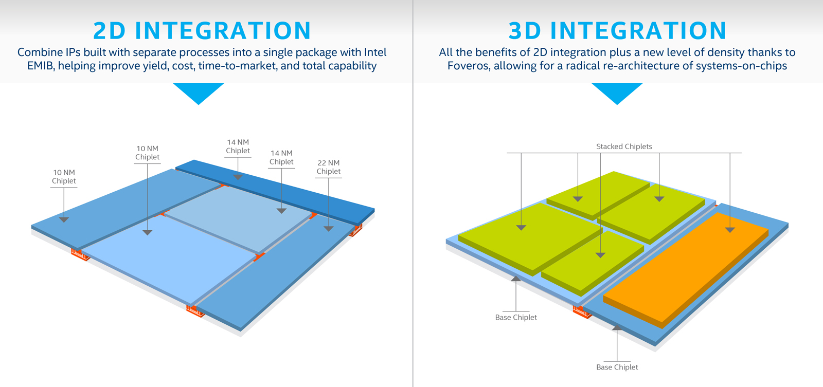
At Architecture Day 2018, Intel demonstrated a new 3D packaging technology it's calling "Foveros." According to Chipzilla, it represents the first time 3D stacking benefits have been applied to logic-on-logic integration. This means that CPU, graphics and AI processors can be assembled vertically atop other components.

Given the emerging IoT industry and the advent of 5G wireless technology, Foveros could play a major role in the development of next-gen small-form factor devices.
The first Foveros product, expected in the second half of 2019, will "combine a high-performance 10nm compute-stacked chiplet with a low-power 22FFL base die." As The Verge highlights, this may be Intel's way of skirting issues it has had with its 10nm manufacturing process:
"Intel suggests it will do something it calls 2D stacking, which is a separation of the various processor components into smaller chiplets, each of which can be manufactured using a different production node. Thus, Intel could deliver nominally 10nm CPUs, which will nonetheless have various 14nm and 22nm chiplet modules within them."
An Intel rep told the publication that Foveros processors will eventually show up in everything "from mobile devices to the data center."
